- 您现在的位置:买卖IC网 > Sheet目录2008 > MAX11201BEUB+T (Maxim Integrated Products)IC ADC 24BIT SRL 13.75SPS 10UMAX
8 ______________________________________________________________________________________
MAX11201
24-Bit, Single-Channel, Ultra-Low-Power, Delta
Sigma ADC with 2-Wire Serial Interface
Pin Description
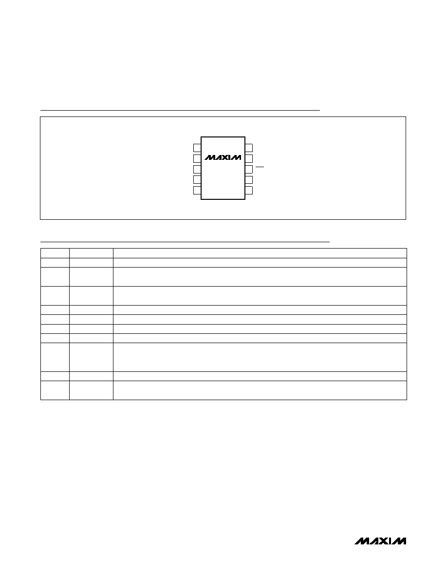
Pin Configuration
+
1
2
3
4
5
10
9
8
7
6
CLK
SCLK
DVDD
AINN
REFN
REFP
GND
MAX11201
MAX
TOP VIEW
AVDD
AINP
RDY/DOUT
PIN
NAME
FUNCTION
1
GND
Ground. Ground reference for analog and digital circuitry.
2
REFP
Differential Reference Positive Input. REFP must be more positive than REFN. Connect REFP to a volt-
age between AVDD and GND.
3
REFN
Differential Reference Negative Input. REFN must be more negative than REFP. Connect REFN to a
voltage between AVDD and GND.
4
AINN
Negative Fully Differential Analog Input
5
AINP
Positive Fully Differential Analog Input
6
AVDD
Analog Supply Voltage. Connect a supply voltage between +2.7V to +3.6V with respect to GND.
7
DVDD
Digital Supply Voltage. Connect a digital supply voltage between +1.7V to +3.6V with respect to GND.
8
RDY/DOUT
Data Ready Output/Serial Data Output. This output serves a dual function. In addition to the serial data
output function, the RDY/DOUT also indicates that the data is ready when the RDY is logic-low. RDY/
DOUT changes on the rising edge of SCLK.
9
SCLK
Serial Clock Input. Apply an external serial clock to SCLK.
10
CLK
External Clock Signal Input. The internal clock shuts down when CLK is driven by an external clock.
Use a 2.4576MHz oscillator (MAX11201A) or a 2.25275MHz oscillator (MAX11201B).
发布紧急采购,3分钟左右您将得到回复。
相关PDF资料
MAX11202BEUB+T
IC ADC 24BIT SRL 13.75SPS 10UMAX
MAX11210EEE+T
ADC 24BIT 4WIRE SPI 16-QSOP
MAX11212BEUB+T
IC ADC 18BIT SRL 13.75SPS 10UMAX
MAX1135BCAP+
IC ADC 16BIT 150KSPS 20-SSOP
MAX1138LEEE+T
IC ADC 10BIT SERIAL 16-QSOP
MAX1159AEUI+
IC ADC 14BIT 135KSPS 28-TSSOP
MAX11602EEE+
IC ADC SERIAL 8BIT 8CH 16-QSOP
MAX11610EEE+T
IC ADC SERIAL 10BIT 12CH 16-QSOP
相关代理商/技术参数
MAX11201EUB+
功能描述:模数转换器 - ADC 24 Bit Sigma Delta ADC RoHS:否 制造商:Texas Instruments 通道数量:2 结构:Sigma-Delta 转换速率:125 SPs to 8 KSPs 分辨率:24 bit 输入类型:Differential 信噪比:107 dB 接口类型:SPI 工作电源电压:1.7 V to 3.6 V, 2.7 V to 5.25 V 最大工作温度:+ 85 C 安装风格:SMD/SMT 封装 / 箱体:VQFN-32
MAX11201EUB+T
功能描述:模数转换器 - ADC 24 Bit Sigma Delta ADC RoHS:否 制造商:Texas Instruments 通道数量:2 结构:Sigma-Delta 转换速率:125 SPs to 8 KSPs 分辨率:24 bit 输入类型:Differential 信噪比:107 dB 接口类型:SPI 工作电源电压:1.7 V to 3.6 V, 2.7 V to 5.25 V 最大工作温度:+ 85 C 安装风格:SMD/SMT 封装 / 箱体:VQFN-32
MAX11202
制造商:MAXIM 制造商全称:Maxim Integrated Products 功能描述:24-Bit, Single-Channel, Ultra-Low-Power, Delta Sigma ADC with 2-Wire Serial Interface
MAX11202_12
制造商:MAXIM 制造商全称:Maxim Integrated Products 功能描述:24-Bit, Single-Channel, Ultra-Low-Power, Delta Sigma ADC with 2-Wire Serial Interface
MAX11202AEUB
制造商:MAXIM 制造商全称:Maxim Integrated Products 功能描述:24-Bit, Single-Channel, Ultra-Low-Power, Delta Sigma ADC with 2-Wire Serial Interface
MAX11202AEUB+
功能描述:模数转换器 - ADC 24-Bit Delta-Sigma RoHS:否 制造商:Texas Instruments 通道数量:2 结构:Sigma-Delta 转换速率:125 SPs to 8 KSPs 分辨率:24 bit 输入类型:Differential 信噪比:107 dB 接口类型:SPI 工作电源电压:1.7 V to 3.6 V, 2.7 V to 5.25 V 最大工作温度:+ 85 C 安装风格:SMD/SMT 封装 / 箱体:VQFN-32
MAX11202AEUB+T
功能描述:模数转换器 - ADC 24-Bit Delta-Sigma RoHS:否 制造商:Texas Instruments 通道数量:2 结构:Sigma-Delta 转换速率:125 SPs to 8 KSPs 分辨率:24 bit 输入类型:Differential 信噪比:107 dB 接口类型:SPI 工作电源电压:1.7 V to 3.6 V, 2.7 V to 5.25 V 最大工作温度:+ 85 C 安装风格:SMD/SMT 封装 / 箱体:VQFN-32
MAX11202BEUB
制造商:MAXIM 制造商全称:Maxim Integrated Products 功能描述:24-Bit, Single-Channel, Ultra-Low-Power, Delta Sigma ADC with 2-Wire Serial Interface